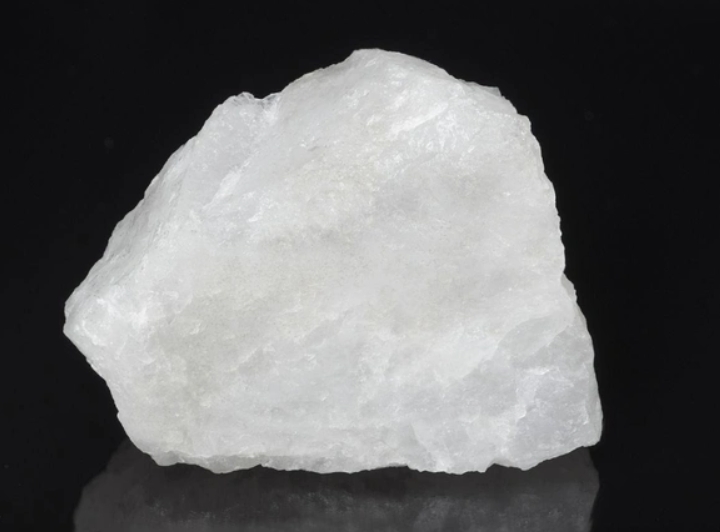
Most PCB enthusiasts, hardware engineers, and substrate R&D professionals share a baseline understanding: a circuit board fundamentally consists of copper foil, fiberglass cloth, and epoxy resin. The copper foil handles conductive traces, the fiberglass builds the structural skeleton, and the resin provides insulation and bonding. However, many overlook a critical material that is invisible and intangible, yet dictates much of a PCB’s overall reliability—micro-silica powder (silica filler).
Unlike copper lines, pads, or solder masks, micro-silica is not visible to the naked eye. It is not individually labeled on layer stackup diagrams, nor does it form an independent board structure.
Instead, it acts as an ultra-fine “mineral aggregate” within the PCB material ecosystem, silently blended into resins, inks, and packaging compounds. Whether a board warps, how stable high-speed signals remain, whether thermal cycling causes delamination or cracking, and how durable the board is in hot, humid environments—all depend heavily on this hidden filler.
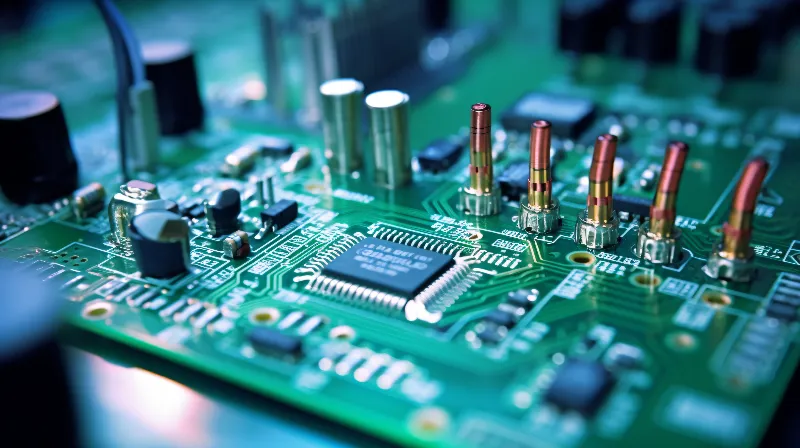
1. Micro-Silica Has No Dedicated Layer—It Blends Into the Material System
A common misconception is trying to locate a dedicated “micro-silica layer” within the PCB stackup structure. In reality, its fundamental logic boils down to a single principle: it is not about where it is placed, but which material it is mixed into.
Micro-silica remains dispersed throughout various polymer systems during processing. Through micro-scale modification, it optimizes three core performance metrics of the board from the ground up: thermal, mechanical, and electrical properties.
In the PCB industry, micro-silica primarily operates in four key areas that directly cover core board reliability:
- Substrate Resin: The foundation of standard substrate systems like FR-4.
- Copper Clad Laminate (CCL) Dielectric Layer: The insulating layer between copper foils, vital for high-speed boards.
- Solder Mask Ink: Commonly known as the PCB green oil layer.
- Chip Packaging Materials: Epoxy Molding Compounds (EMC) for BGA, CSP, and similar packages.
Substrate Resin
The core combination of standard FR-4 substrates consists of fiberglass cloth as the structural frame and epoxy resin as the bonding matrix.
Fiberglass offers high strength and dimensional stability, but cannot absorb or fill resin directly on its own. Resin provides flexibility and excellent electrical insulation, yet suffers from a fatal flaw: an extremely high Coefficient of Thermal Expansion (CTE). With slight temperature fluctuations, the resin expands and contracts significantly. This behavior drives most baseline PCB failures:
- Warping, deformation, and dimensional drift after reflow soldering or thermal cycling.
- Continuous accumulation of interlaminar stress, leading to potential delamination.
- Elevated risk of fatigue cracking around plated through-holes (PTH) and microvias.
- Dielectric thickness fluctuations that cause impedance drift in high-speed boards.
Adding micro-silica offsets these inherent flaws of the resin. Ultra-fine, highly stable micro-silica particles disperse uniformly throughout the resin matrix. This process effectively incorporates rigid mineral aggregate into soft resin, significantly reducing the overall CTE and locking in dimensional stability.
Simply put, raw resin acts as an easily deformed “soft material.” Blending in micro-silica transforms it into a temperature-resistant, expansion-resistant “composite rigid structure,” addressing board instability at its root cause.

Copper Clad Laminate (CCL) Dielectric Layer
When designing high-speed PCBs, engineers typically focus on optimizing trace widths, spacing, copper weight, layer stackups, and impedance targets. Yet many overlook a fundamental truth: while high-speed signals travel along copper traces, the electromagnetic fields propagate entirely through the dielectric layer. If the dielectric material is unstable, even the most precise trace routing will fall short.
In CCL dielectric layers for high-speed/high-frequency boards, 5G communications, automotive electronics, and IC substrates, spherical, ultra-fine, high-purity micro-silica serves as a primary modifying filler. Its value focuses on two main dimensions:
- Achieving High Consistency in Dielectric Performance:Pure resin systems are prone to performance variations driven by production batches, processing techniques, and thermal history. Uniformly dispersed micro-silica suppresses resin volatility. This consistency ensures uniform dielectric parameters across different regions and batches, eliminating impedance drift and signal distortion caused by material variations.
- Controlled Thermal Stress Relief and Enhanced Long-Term Durability:High-speed boards face simultaneous challenges from signal transmission, heat generation, and ambient temperature swings. Repeated thermal expansion and contraction continuously pull at the copper foil and dielectric interfaces. Over time, this leads to failures like delamination, micro-cracks, and interface detachment.By stabilizing the thermomechanical properties of the dielectric layer, micro-silica minimizes temperature-induced dimensional changes. As a result, high-speed boards maintain controlled performance during long-term thermal cycling and under complex operating conditions.
Solder Mask Ink
Solder mask is often regarded as merely a protective insulating paint designed to prevent short circuits and oxidation. In truth, the solder mask serves as the PCB’s first line of defense against the external environment. It carries multiple responsibilities, including insulation, corrosion resistance, wear resistance, moisture resistance, and anti-aging properties.
High-quality solder mask inks incorporate micro-silica to target surface durability:
- Enhances Surface Hardness Post-Curing: Improves scratch resistance and mechanical wear resistance, preventing surface damage during manufacturing and assembly.
- Boosts Chemical Corrosion Resistance: Shields against erosion caused by fluxes, cleaning agents, and corrosive moisture.
- Optimizes Ink Printing Leveling and Curing Stability: Reduces processing defects such as voids, pinholes, and flaking.
Many early PCB failures stem not from copper line breakage or dielectric breakdown, but from the premature aging and degradation of the solder mask. Once this shield breaks down, moisture and contaminants invade the board’s interior, triggering cascading faults. The micro-silica concealed within the ink serves as an invisible barrier extending PCB lifespan.
Chip Packaging Materials
While micro-silica acts as a “reinforcing filler” in the previous three scenarios, it upgrades to a core primary material in Epoxy Molding Compounds (EMC) for BGA and CSP chip packaging—often accounting for up to 70% or more of the formulation.
This high loading ratio is not meant for cost reduction; it is an absolute necessity under high-stress chip operating conditions. Chip packaging systems demand extreme thermal stress management and coefficient matching: raw resin has a high CTE, whereas silicon dies and substrates possess extremely low CTEs. Temperature changes produce significant thermal expansion mismatches, generating massive internal stresses.
Micro-silica’s high stability drastically lowers the overall CTE of the packaging compound. This allows the thermal expansion of the encapsulation layer, chip, and substrate to closely align with one another.
This alignment mitigates three major failure modes at their root:
- Package cracking caused by thermal shock.
- Delamination at the interfaces between the package, substrate, and die.
- Stress concentration and fatigue failure at solder joints.
Under long-term high-operating temperatures and repeated thermal cycling, high-content micro-silica provides essential reliability for chip packaging.
Golden Synergy
People often confuse the roles of fiberglass cloth and micro-silica. In reality, they form a complementary dynamic duo:
- Fiberglass Cloth = The PCB’s Structural Skeleton: Provides overall mechanical strength and builds the baseline structure, determining whether the board can hold its shape under load.
- Micro-Silica = Micro-Fine Aggregate: Fills microscopic voids within the resin to optimize its thermal and mechanical performance. It compensates for the anisotropic drawbacks of woven fiberglass, ensuring the board remains stable, durable, and long-lasting.
In summary: Fiberglass handles structural strength, while micro-silica stabilizes performance, resists aging, and withstands thermal cycling.
As the industry transitions toward halogen-free eco-friendly laminates, traditional halogen-containing resin systems are being replaced. However, while these eco-friendly upgrades comply with environmental regulations, new halogen-free resins often suffer from reduced heat resistance, lower thermal stability, and narrower processing windows. This makes board reliability vulnerable.
Micro-silica functions as a vital performance stabilizer for halogen-free laminates. By precisely tuning the filler ratio, engineers can optimize thermal expansion, heat resistance, and mechanical strength in halogen-free resin systems. This ensures eco-friendly materials meet strict reliability thresholds for high-end electronics.
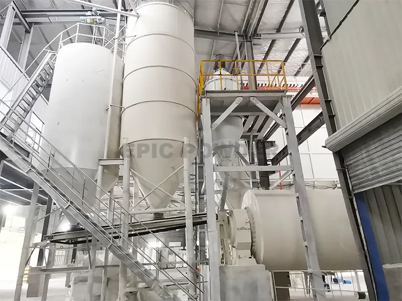
2. Core Engineering Logic: How Micro-Silica Elevates PCB Reliability
Setting aside complex application scenarios, the value of micro-silica boils down to three core engineering principles:
- Lowers CTE to Suppress Deformation Impulses:Resin thermal expansion and contraction cause most PCB failures. Adding micro-silica significantly reduces the composite material’s CTE, minimizing or eliminating deformation under changing temperatures.
- Balances Deformation to Relieve Thermal Stress:Mismatches in material expansion create interface stresses that accumulate into micro-cracks, delamination, and peeling. Micro-silica ensures more uniform and controllable material deformation, stopping stress accumulation at the source.
- Locks In Performance to Prevent Parameter Drift:Whether maintaining impedance stability on high-speed boards, controlling board warping, or ensuring long-term reliability in hot and humid environments, the underlying goal is consistent long-term performance. As a stabilizing filler, micro-silica resolves the performance volatility inherent in resin systems.
3. Real Value Often Lies Out of Sight
When inspecting a PCB, attention naturally falls first on traces, pads, layer counts, and surface finish. However, whether a board withstands high-temperature reflow, millions of thermal cycles, long-term high-speed signal transmission, and harsh moisture environments depends on elements far beyond visible structures.
Concealed within resins, inks, and packaging compounds, micro-silica works silently out of sight. With every temperature swing, stress pull, and high-frequency signal pass, it quietly upholds the baseline of PCB reliability. Visible parts form the structure, but invisible materials define the performance.

“Thanks for reading. I hope my article helps. Please leave a comment down below. You may also contact Zelda online customer representative for any further inquiries.”
— Posted by Emily Chen